Ion Etching System
Technical Information
What is Ion Etching System?
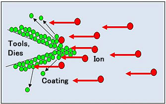
Ion etching is a type of dry etching technique that physically processes an object by irradiating it with ionized atoms.
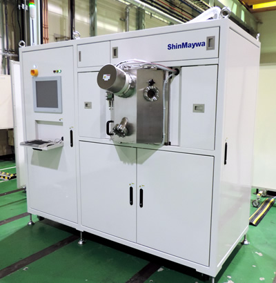
This device functions as an ion beam etching system, enabling high-precision processing and precise etching.
Our company utilizes its unique ion beam etching technology to develop ion etching equipment for cutting tools, molds, and various parts.
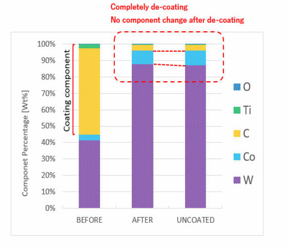
The film removal process allows for the reuse of the substrate, contributing to cost reduction and efficient resource utilization.
There is a de-coating method using chemical but it may cause damages to a substrate and uses different chemical liquids depending on coating types.
When using hard metal alloy as a substrate, its component, cobalt is melted by chemical and the surface gets damaged, therefore it is considered to be difficult to reuse.
Our dry etching equipment is an effective, environmentally friendly film removal technology that does not use chemicals.
By using a dry process that does not involve the use of chemicals, we achieve low-damage processing that minimizes damage to the substrate surface.
In addition to film removal, we can also handle high-precision processing such as microburr removal, tip shape correction, microfabrication, and nanofabrication.
Advantages
- Reusing the substrate by removing the film contributes to reducing substrate costs and processing costs.
- It can also be used for recovering defective products in the film deposition process and for pre-treatment before re-deposition.
- Because it does not use chemicals, wastewater treatment is unnecessary, reducing the environmental impact. It can also be used for surface cleaning applications.
- Uniform etching using an ion beam enables stable processing of complex shapes and precision parts.
- It is also expected to have applications in fields requiring highly anisotropic etching.
ShinMaywa's Ion Etching System
Our lineup ranges from compact models for high-mix, low-volume production to high-performance models, catering to various dry etching equipment applications.
We will propose the most suitable ion etching equipment and microfabrication equipment according to the target material and processing requirements.
System Specifications and De-coating Object
| System specifications | ||
|---|---|---|
| Series | IE series | cIE series |
| Size | W 2,300mm | W 900mm |
| D 1,400mm | D 1,200mm | |
| H 2,350mm | H 1,700mm | |
| Weight | Approx. 1,600kg | Approx. 700kg |
| Gas | Ar, O2 | Ar, O2 |
| Ion guns | 4, 6, 8 sources | 3, 5 sources |
| Max elec. consumption | 19-31kVA | 9-12kVA |
| De-coating object (coating) | |
|---|---|
| Carbon | Diamond coating, DLC |
| Nitriding | TiN, TiAlN, AlN, AlCrN, TiCrN, CrN etc. |
| Metal | Si, Cr etc. |
Application examples
Coating tools on carbide substrates
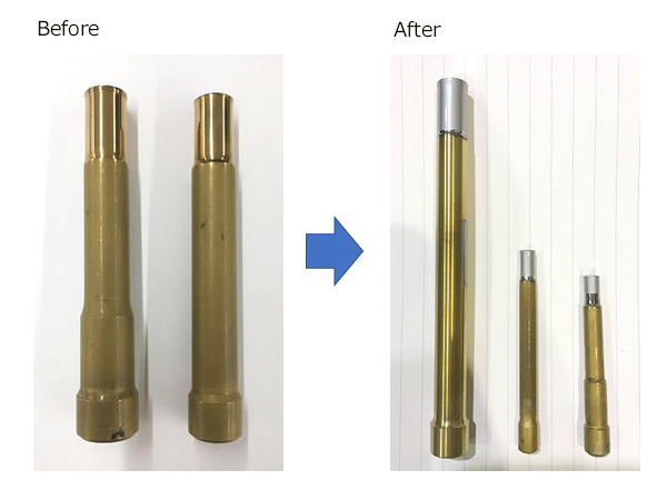
- By applying a low-damage processing technique to ultra-hard materials, we achieve both coating removal and base material reuse.
- High-precision machining allows for film removal while maintaining the blade tip shape and dimensional accuracy.
- In addition to cemented carbide substrates, it can be applied to a wide range of materials, including ceramics and metal parts.
De-coating Example of Carbide Endmill
AlCrN series
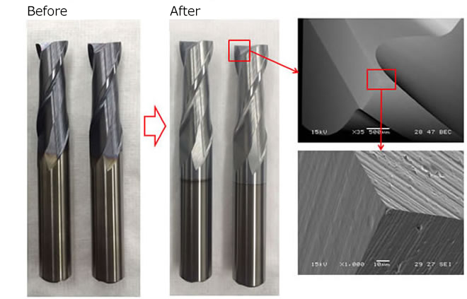
Substrate:Carbide
Coating type:AlCrN(2-3μm)
De-coating Example of Carbide Hob Cutter
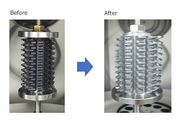
Movie
[Coating removal and sharpening!] ShinMaywa Industries' Ion Etching System
De-coating Example of Carbide Punch
Movie
[ShinMaywa 's Ion Etching System] ★ Minimizes damage to substrates and enables the reuse of carbide tools, etc.!
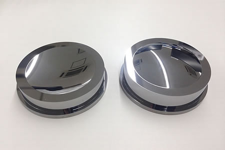
Lens mold
Applications include etching optical components and precision machining of lens molds.
It is also expected to be used in surface preparation processes before the formation of fine patterns.
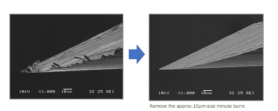
Deburring effect of injection needle
We utilize microfabrication technology to remove minute burrs from precision parts such as hypodermic needles.
This is expected to stabilize quality through uniform etching.
Expected future applications
- Microstructure formation and surface treatment in MEMS processing.
- As a complementary application to semiconductor etching equipment, it is used for precision etching in research and development and prototyping processes.
- Applications include oxide film removal and pre-deposition cleaning processes.
- Applications to electrode pattern formation and thin film patterning processes.
- This field involves the manufacturing of advanced devices requiring high-aspect-ratio processing and fine pattern formation.
- High-precision surface machining for optical components and functional materials.
Contact Information
For product inquiries, please click the button below
Search for other products and services
ShinMaywa INSIGHT